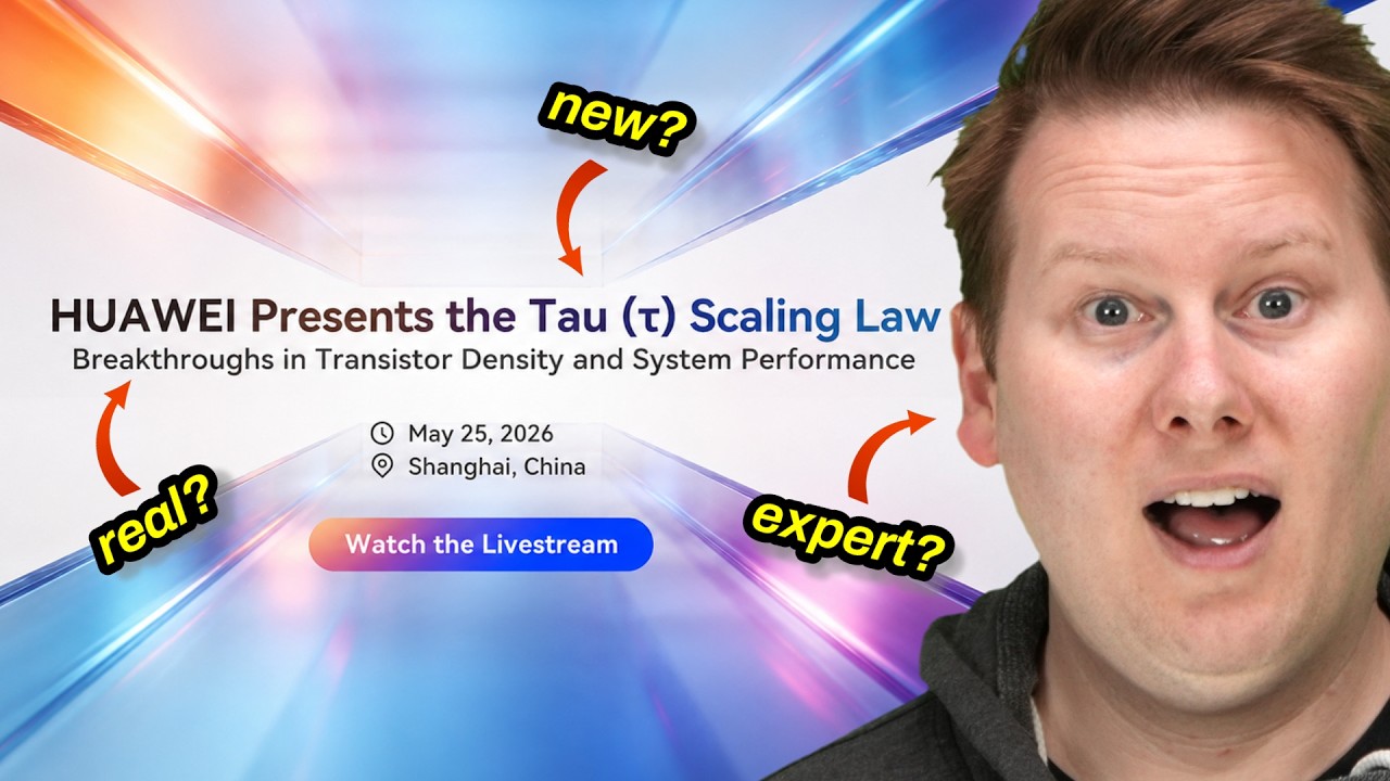
Huawei recently announced ambitious plans to produce 1.4 nanometer class chips by 2031 despite lacking access to advanced EUV lithography tools due to US sanctions. To achieve this, Huawei introduced a new concept called “tow scaling,” which redefines traditional Moore’s Law by focusing on holistic system improvements rather than just transistor density scaling. A key technique they are developing is “logic splitting” or “logic folding,” a form of 3D stacking where multiple logic layers are bonded together at very fine pitches, potentially below two microns, which could enhance performance and efficiency despite the limitations in lithography.
The tow scaling concept essentially broadens the scope of semiconductor progress beyond just shrinking transistor sizes. While Moore’s Law traditionally emphasizes geometric scaling and transistor density, tow scaling includes improvements in device efficiency, packaging, circuit design, and system-level optimization. However, experts argue that this is more a rebranding or refocusing rather than a revolutionary breakthrough, as the industry has long pursued similar holistic approaches. Huawei claims to have already produced hundreds of chips using this philosophy, but this approach is not unique and has been part of semiconductor development for decades.
Logic folding or logic stacking involves bonding multiple chip layers together using advanced hybrid bonding techniques. This method is similar to what companies like AMD and Intel have explored with chiplet architectures and 3D stacking, but Huawei aims to push the bonding pitch to sub-two microns, which would be a significant technical achievement. Challenges include managing the increased resistance and capacitance at the bonding interfaces, ensuring high yield in mass production, and synchronizing timing across layers. The approach also raises questions about thermal management, as stacking logic chips increases heat density, which is particularly problematic in power-constrained devices like smartphones.
Thermal issues are a major concern with Huawei’s proposed 3D logic-on-logic stacking. Unlike memory-on-logic stacking, which is more common, stacking active logic layers generates significant heat on both sides of the chip stack, complicating heat dissipation. Efficient cooling solutions are limited in smartphones, and Huawei has yet to provide detailed strategies for addressing these thermal challenges. Experts note that thermal management is a current, not future, challenge and that overcoming it is critical for the viability of such advanced 3D chip architectures.
Overall, while Huawei’s announcements have generated significant media attention and speculation about bypassing US sanctions through innovative chip design, the underlying technologies and concepts are extensions of existing semiconductor research and development trends. The real breakthrough would be in successfully implementing these techniques at scale with high yield and manageable thermal profiles. The presentation’s language and style suggest possible AI assistance in drafting, and some claims remain to be independently verified. The industry will be watching closely to see if Huawei can translate these ideas into competitive, mass-produced chips despite the constraints imposed by sanctions.