The main bottleneck in AI computing is not raw computational power but the limited data transfer speed between chips, constrained by chip geometry and interconnect area. Advances like 2.5D packaging and especially hybrid bonding, which directly fuses copper interconnects for denser, lower-resistance connections, are crucial innovations addressing this challenge to enhance performance in AI workloads.
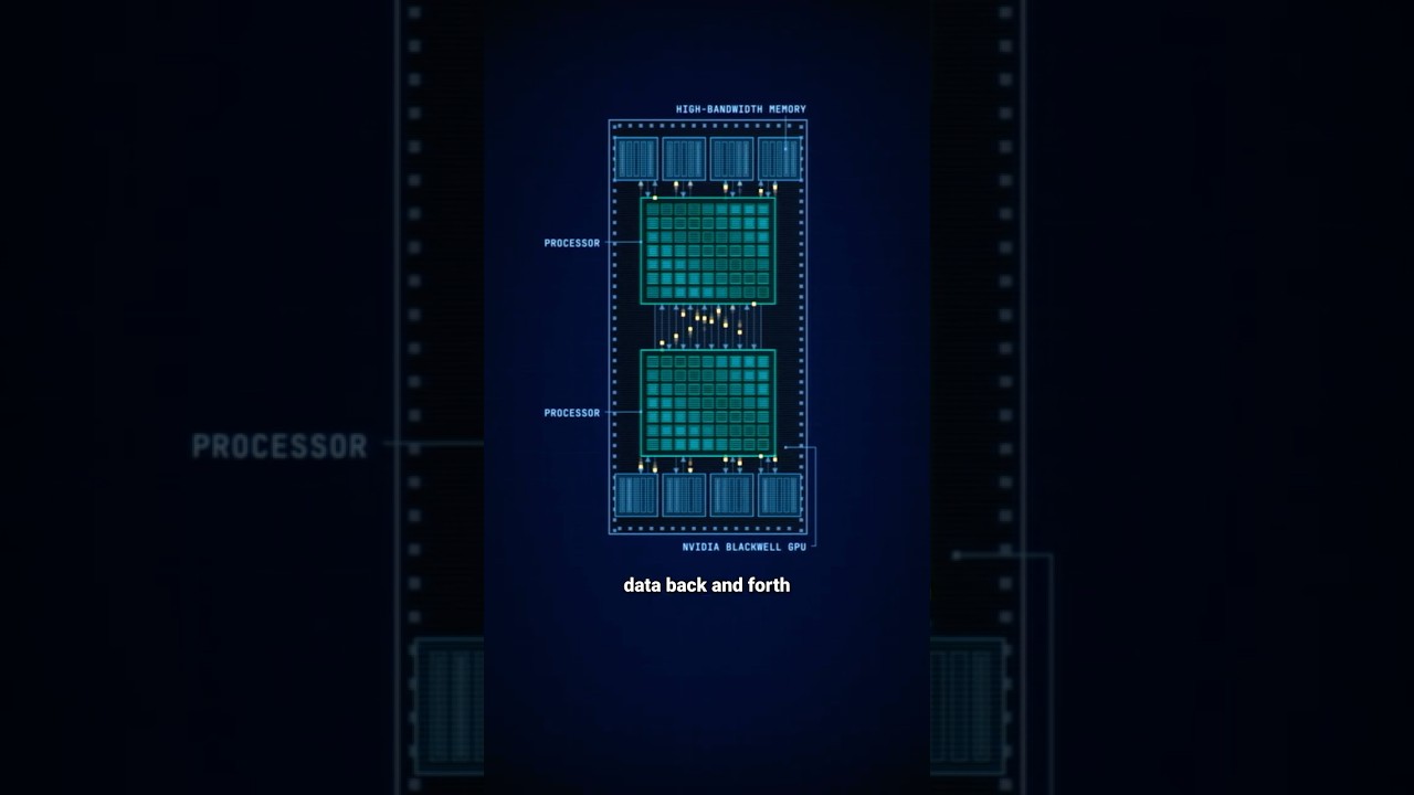
Modern computers are composed of multiple specialized parts, each optimized for specific tasks. For instance, Nvidia’s Blackwell data center GPU integrates two large processor chips surrounded by high bandwidth memory stacks. These chips must continuously exchange data, and in AI workloads, the speed of this data transfer often becomes the bottleneck rather than the raw computational power itself.
A fundamental challenge in chip design is the area versus perimeter problem. When the size of a chip is doubled in both width and length, its area—and thus the number of transistors—increases fourfold, but the edge length available for inter-chip connections only doubles. This means that as chips become denser and more powerful, their ability to move data around does not scale proportionally, limiting overall performance.
To address this issue, the semiconductor industry has developed various packaging technologies. Initially, chips were placed side by side and connected with wires running along their edges. To increase communication density, an interposer—a shared silicon substrate—was introduced, allowing multiple chips to sit on it and communicate through wiring embedded within the interposer. This approach is known as 2.5D packaging.
Another advancement is bonding chips directly to each other to shorten connection lengths. Early methods used solder bumps, which were bulky and increased electrical resistance. A more advanced technique called hybrid bonding eliminates solder bumps by directly fusing the copper interconnects of adjacent chips. This method allows for much denser and lower-resistance connections, improving data transfer speeds between chips.
Hybrid bonding has only recently entered volume manufacturing due to the technical challenges involved, such as precise alignment and defect management. By overcoming these hurdles, hybrid bonding represents a significant step forward in chip packaging technology, helping to alleviate the data transfer bottleneck in modern high-performance computing systems, especially those used for AI workloads.
Useful Links